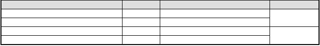
4.Absolute maximum ratings
Item
Symbol
Standard
Unit
Power voltage VDD-VSS
0 - 7.0
V
Input voltage VIN
VSS - VDD
Operating temperature range VOP
-20 - +70
-30 - +80
℃
Storage temperature range VST
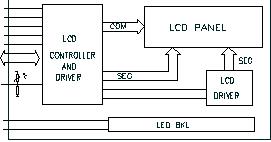
5.Block diagram
6.Interface pin description
Pin no.
Symbol
External
connection
Function
1 GND
2 VDD Power supply for logic (+3.3V) for LCM Power supply
Signal ground for LCM (GND)
3 V0 Contrast adjust
4 RS MPU Register select signal
5 R/W MPU Read/write select signal
6 E MPU Operation (data read/write) enable signal
7~10 DB0~DB3 MPU
Four low order bi-directional three-state data bus lines.
Used for data transfer between the MPU and the LCM.
These four are not used during 4-bit operation.
11~14 DB4~DB7 MPU
Four high order bi-directional three-state data bus lines.
Used for data transfer between the MPU
15 LED+ LED BKL power
16 LED- Power supply for BKL supply
Power supply for BKL


发布紧急采购,3分钟左右您将得到回复。
相关PDF资料
NHD-0216K1Z-FL-GBW
LCD MOD CHAR 2X16 Y/G TRANSFL
NHD-0216K1Z-FL-YBW
LCD MOD CHAR 2X16 Y/G TRANSFL
NHD-0216K1Z-FSA-FBW-L
LCD MOD CHAR 2X16 AMB TRANSFL
NHD-0216K1Z-FSA-GBW-L
LCD MOD CHAR 2X16 AMB TRANSFL
NHD-0216K1Z-FSB-FBW-L
LCD MOD CHAR 2X16 BLUE TRANSFL
NHD-0216K1Z-FSB-GBW-L
LCD MOD CHAR 2X16 BLUE TRANSFL
NHD-0216K1Z-FSO-FBW-L
LCD MOD CHAR 2X16 ORN TRANSFL
NHD-0216K1Z-FSO-GBW-L
LCD MOD CHAR 2X16 ORN TRANSFL
相关代理商/技术参数
NHD-0216HZ-FSW-GBW-3V3C
功能描述:LCD字符显示模块与配件 STN- GRAY Transfl 65.5 x 36.7 RoHS:否 制造商:Lumex 显示模式:Transflective 字符计数 x 行:16 x 2 特点: 流体类型:STN 接口: 背景色: 工作温度范围:- 20 C to + 70 C 封装:Bulk
NHD-0216K1Z-FL-GBW
功能描述:LCD字符显示模块与配件 STN- GRAY Transfl 80.0 x 36.0 RoHS:否 制造商:Lumex 显示模式:Transflective 字符计数 x 行:16 x 2 特点: 流体类型:STN 接口: 背景色: 工作温度范围:- 20 C to + 70 C 封装:Bulk
NHD-0216K1Z-FL-YBW
功能描述:LCD字符显示模块与配件 STN- Y/G Transfl 80.0 x 36.0 RoHS:否 制造商:Lumex 显示模式:Transflective 字符计数 x 行:16 x 2 特点: 流体类型:STN 接口: 背景色: 工作温度范围:- 20 C to + 70 C 封装:Bulk
NHD-0216K1Z-FS
制造商:NEWHAVEN 制造商全称:NEWHAVEN 功能描述:Character Liquid Crystal Display Module
NHD-0216K1Z-FS(RGB)-FBW
功能描述:LCD字符显示模块与配件 FSTN (+) Transfl 80.0 x 36.0 RoHS:否 制造商:Lumex 显示模式:Transflective 字符计数 x 行:16 x 2 特点: 流体类型:STN 接口: 背景色: 工作温度范围:- 20 C to + 70 C 封装:Bulk
NHD-0216K1Z-FS(RGB)-FBW-REV1
功能描述:LCD字符显示模块与配件 FSTN (+) Transfl 80.0 x 36.0 RoHS:否 制造商:Lumex 显示模式:Transflective 字符计数 x 行:16 x 2 特点: 流体类型:STN 接口: 背景色: 工作温度范围:- 20 C to + 70 C 封装:Bulk
NHD-0216K1Z-FSA-FBW-L
功能描述:LCD字符显示模块与配件 FSTN (+) Transfl 80.0 x 36.0 RoHS:否 制造商:Lumex 显示模式:Transflective 字符计数 x 行:16 x 2 特点: 流体类型:STN 接口: 背景色: 工作温度范围:- 20 C to + 70 C 封装:Bulk
NHD-0216K1Z-FSA-GBW-L
功能描述:LCD字符显示模块与配件 STN- GRAY Transfl 80.0 x 36.0 RoHS:否 制造商:Lumex 显示模式:Transflective 字符计数 x 行:16 x 2 特点: 流体类型:STN 接口: 背景色: 工作温度范围:- 20 C to + 70 C 封装:Bulk
